全国咨询热线
全国咨询热线

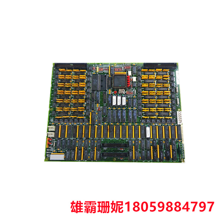
GE的DS200TCDAG1BDB印刷电路板是该公司Speedtronic Mark V系统中使用的数字I/O板。Mark V是用于工业蒸汽和燃气轮机系统的第三代三重模块化冗余管理系统。AX Control 努力维护所有通用电气 Speedtronic 更换零件的现有库存,以便我们能够更快地满足您对这些难以找到的零件的需求。
DS200TCDAG1BDB用作触点输入和继电器输出的接口。软件配置将有助于解决这些问题。
DS200TCDAG1BDB 印刷电路板(Printed Circuit Board,PCB)是一种用于电子设备的电路板,它通过印刷技术在绝缘材料上形成电路图案。
PCB 的制造过程通常包括以下步骤:
1. 设计:使用电路设计软件设计电路板的电路布局。
2. 制版:将设计好的电路布局转化为光刻版,用于印刷电路图案。
3. 印刷:使用印刷技术将电路图案印刷在绝缘材料上。
4. 蚀刻:使用蚀刻技术将不需要的铜箔蚀刻掉,留下需要的电路图案。
5. 钻孔:在电路板上钻出需要的孔洞,用于连接元件和布线。
6. 插件:将电子元件插入电路板上的孔洞中。
7. 焊接:使用焊接技术将元件与电路板连接起来。
8. 测试:对电路板进行测试,确保其正常工作。
DS200TCDAG1BDB PCB 广泛应用于各种电子设备中,如计算机、手机、电视机、游戏机等。它可以实现电子元件之间的连接和布线,提高电子设备的可靠性和稳定性。
总之,DS200TCDAG1BDB 印刷电路板是一种用于电子设备的电路板,它通过印刷技术在绝缘材料上形成电路图案。它的制造过程包括设计、制版、印刷、蚀刻、钻孔、插件、焊接和测试等步骤。PCB 广泛应用于各种电子设备中,提高了电子设备的可靠性和稳定性。
GE's DS200TCDAG1BDB printed circuit board is the digital I/O board used in the company's Speedtronic Mark V system. The Mark V is the third generation triple modular redundancy management system for industrial steam and gas turbine systems. AX Control strives to maintain an existing inventory of all GE Speedtronic replacement parts so that we can more quickly meet your needs for these hard-to-find parts.
The DS200TCDAG1BDB is used as an interface between contact input and relay output. Software configuration will help solve these problems.
The DS200TCDAG1BDB Printed Circuit Board (PCB) is a circuit board for electronic devices that forms a circuit pattern on an insulating material by printing technology.
The manufacturing process of a PCB usually includes the following steps:
1. Design: Use circuit design software to design the circuit layout of the circuit board.
2. Plate making: The designed circuit layout is converted into light engraving plate for printing circuit patterns.
3. Printing: The circuit pattern is printed on the insulation material using printing technology.
4. Etching: Use etching technology to etch away the unwanted copper foil, leaving the required circuit pattern.
5. Drilling: Drill out the required holes on the circuit board for connecting components and wiring.
6. Plug-in: Insert electronic components into holes in the circuit board.
7. Welding: Use welding technology to connect the components to the circuit board.
8. Test: Test the circuit board to ensure that it works properly.
DS200TCDAG1BDB PCB is widely used in various electronic devices, such as computers, mobile phones, TV sets, game consoles and so on. It can realize the connection and wiring between electronic components and improve the reliability and stability of electronic devices.
In short, the DS200TCDAG1BDB printed circuit board is a circuit board for electronic devices, which forms circuit patterns on insulating materials through printing technology. Its manufacturing process includes steps such as design, plate making, printing, etching, drilling, plug-in, welding and testing. PCB is widely used in a variety of electronic equipment, improve the reliability and stability of electronic equipment.
| ABB | G3FCb |
| ABB | HENF458568R1 |
| ABB | G3FD |
| ABB | HENF452692R1 |
| ABB | G3FE |
| ABB | HENF452697R1 |
| ABB | HENF452750R1 |
| ABB | E3EP |
| ABB | HENF315276R1 |
| ABB | E3ES |
| ABB | E5EAA |
| ABB | HENF105240R1 |
| ABB | G3EA |
| ABB | HENF315754R1 |
| ABB | G3EB |
| ABB | HENF315768R1 |
雄霸工控

微信二维码
Copyright © 2022-2024 厦门雄霸电子商务有限公司 版权所有 备案号:闽ICP备14012685号-33