全国咨询热线
全国咨询热线

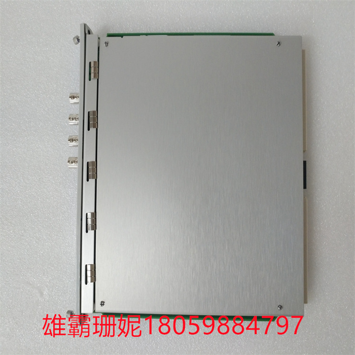
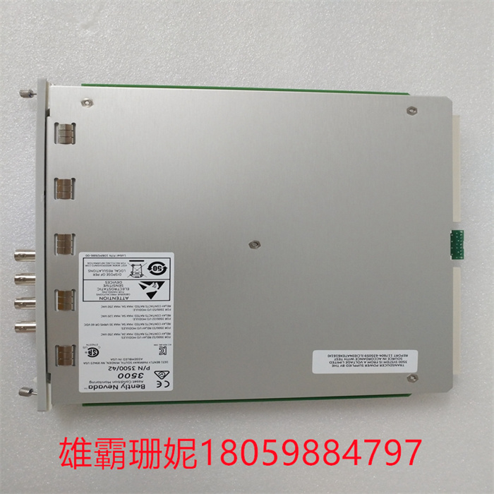
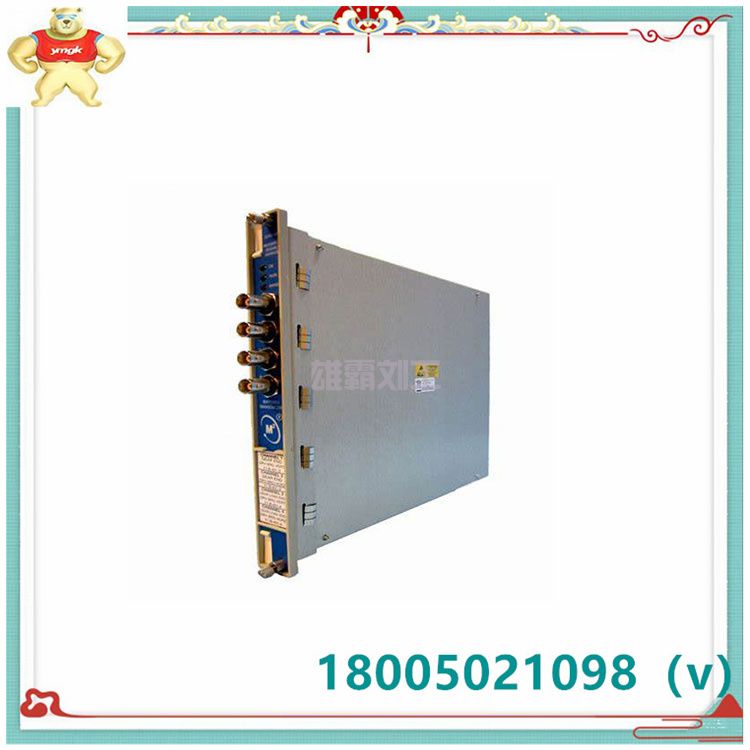
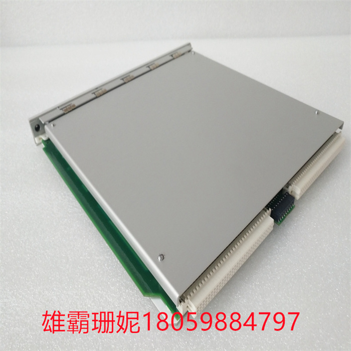
BENTLY 3500/42M 176449-02 监测模块处理器
BENTLY 3500/42M 176449-02 监测模块处理器

本特利3500/42M 176449-02轴振动模块现货供应。美国本特利bently nevada轴振动模块型号3500/42M 176449-02广泛应用发电、化工、冶金、石油厂、水泥厂、冶金厂、造纸厂、机械等各种不同的工业部门。3500/42M 176449-02型号是是本特利bently3500振动监测模块之一,又称3500/42M 位移/速度加速度监测它可以监测大型旋转机械的振动,如汽轮机、压缩机,水泵等的轴振、瓦振、胀差、摆度、偏心、轴向位移,机壳膨胀等。bently3500的TSI监测需配套以下模块才可以运行,3500/01软件,3500/05 系统框架,3500/15电源,3500/20框架接口模块3500/22M 带有TDI的框架接口模块,3500/32四通道继电器模块,3500/33继电器模块,3500/50 转速模块,3500/53超速检测模块,3500/92通讯网关,3500/93 LCD 显示装置。
CPU缓存的早期例子包括地图集2[3]和IBM System/360 85型[4]20世纪60年代。第一个使用缓存的CPU只有一级缓存;与后来的一级缓存不同,它没有分成L1d(用于数据)和L1i(用于指令)。拆分L1缓存始于1976年IBM 801CPU,[5][6]在20世纪80年代后期成为主流,并在1997年以ARMv5TE进入嵌入式CPU市场。2015年,甚至低于美元的SoC也瓜分了L1的缓存。它们还有L2高速缓存,对于更大的处理器,还有L3高速缓存。L2缓存通常不会被拆分,而是充当已经拆分的L1缓存的公共存储库。的每个核心多核处理器拥有专用的L1缓存,通常不在内核之间共享。L2高速缓存和更高级的高速缓存可以在核之间共享。L4高速缓存目前并不常见,通常处于开启状态(一种形式的)动态随机存取存储器(DRAM),而不是在静态随机存取存储器(SRAM),在单独的管芯或芯片上(例外地,形式,eDRAM用于所有级别的缓存,下至L1)。历史上L1也是如此,虽然更大的芯片允许集成它和一般所有高速缓存级别,最后一级可能除外。每个额外级别的缓存往往更大,优化方式也不同。
高速缓存(类似于历史上的RAM)的大小通常是2、4、8、16等的幂。KiB;到什么时候弹子大小(即对于较大的非L1),很早就打破了这种模式,允许更大的缓存,而不必被迫采用大小加倍的模式,例如英特尔酷睿2双核处理器2008年4月推出3 MiB L2高速缓存。然而,很久以后,对于L1的尺寸来说,这仍然只在KiB的小部分地区有效IBM zEC12从2012年是一个例外,获得异常大的96 KiB L1数据缓存的时间,例如IBM z13具有96个KiB L1指令高速缓存(和128个KiB L1数据高速缓存),[7]和英特尔冰湖基于2018年的处理器,拥有48个KiB L1数据高速缓存和48个KiB L1指令高速缓存。2020年,一些英特尔凌动处理器CPU(最多24个内核)具有4.5 MiB和15 MiB缓存大小(的倍数)。
BENTLY 3500/42M 176449-02 监测模块处理器
Bentley 3500/42M 176449-02 shaft vibration module available from stock. Bentley bently nevada shaft vibration module Model 3500/42M 176449-02 widely used in power generation, chemical, metallurgy, petroleum plants, cement plants, metallurgical plants, paper mills, machinery and other different industrial sectors. Model 3500/42M 176449-02 is one of Bentley bently3500 vibration monitoring modules, also known as 3500/42M displacement/velocity acceleration monitoring it can monitor the vibration of large rotating machinery, such as steam turbines, compressors, water pumps and other axial vibration, tile vibration, expansion, swing, eccentrics, axial displacement, housing expansion and so on. bently3500's TSI monitoring requires the following modules to operate: 3500/01 software, 3500/05 system frame, 3500/15 power supply, 3500/20 frame interface module 3500/22M frame interface module with TDI, 3500/32 four-channel relay module, 3500/32 3500/33 relay module, 3500/50 speed module, 3500/53 speed detection module, 3500/92 communication gateway, 3500/93 LCD display device.
Early examples of CPU caches include Atlas 2[3] and IBM System/360 Model 85 [4] from the 1960s. The first CPU to use the cache had only one level of cache; Unlike later level-1 caches, it is not split into L1d(for data) and L1i(for instructions). Split L1 caches began with the IBM 801CPU in 1976, [5][6] became mainstream in the late 1980s, and entered the embedded CPU market with the ARMv5TE in 1997. In 2015, even subdollar SoCs carved up L1's cache. They also have L2 caches, and for larger processors, L3 caches. L2 caches are not usually split, but instead act as a common repository for the L1 caches that have already been split. Each core multi-core processor has a dedicated L1 cache that is not usually shared between cores. L2 caches and more advanced caches can be shared between cores. L4 caches are currently uncommon and are usually on (a form of) dynamic random access memory (DRAM), rather than on static random access memory (SRAM), on separate cores or chips (with the exception, form, eDRAM is used for all levels of caching, down to L1). The same has historically been true of L1, although larger chips have allowed it and generally all cache levels to be integrated, with the possible exception of the last level. Each additional level of cache tends to be larger and optimized differently.
The size of a cache (similar to RAM historically) is usually a power of 2, 4, 8, 16, etc. KiB; When it came to pin size (i.e., for larger non-L1), this pattern was broken very early, allowing for larger caches without being forced to adopt a size doubling pattern, such as the 3 MiB L2 cache introduced by Intel Core 2 Duo processors in April 2008. However, much later, for the size of L1, this was still only valid in a small area of KiB. The IBM zEC12 from 2012 was an exception, acquiring an unusually large 96 KiB L1 data cache for the time being. For example, the IBM z13 has 96 KiB L1 instruction caches (and 128 KiB L1 data caches), [7] and Intel Ice Lake's 2018 based processor has 48 KiB L1 data caches and 48 KiB L1 instruction caches. In 2020, some Intel Atom processor cpus (up to 24 cores) have 4.5 MiB and 15 MiB cache sizes (multiples).
BENTLY 3500/42M 176449-02 监测模块处理器
| BENTLY | 3500/32 125712-01 |
| BENTLY | 3500/92 |
| BENTLY | 136188-01 |
| BENTLY | 125720-01 |
| BENTLY | 3500/91-01-01(161204-01+161216-01) |
| BENTLY | 125800-01 |
| BENTLY | 3500/45 176449-04 |
| BENTLY | 3500/15 127610-01 |
| BENTLY | 125840-01 |
| BENTLY | 3500/25 125792-01 |
| BENTLY | 3500/05-01-03-00-00-00 |
| BENTLY | 128229-01 |
| BENTLY | 128229-01 |
| BENTLY | 128229-01 |
| BENTLY | 3500/42M 140734-02 |
| BENTLY | 3500/33-01-00 |
| BENTLY | 128229-01 |
| BENTLY | 135137-01 |
| BENTLY | 133396-01 |
雄霸工控

微信二维码
Copyright © 2022-2024 厦门雄霸电子商务有限公司 版权所有 备案号:闽ICP备14012685号-33