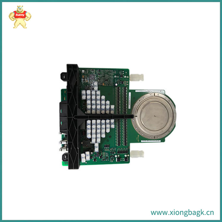
当IGCT工作在导通状态时,是一个像晶闸管一样的正反馈开关,其特点是携带电流能力强和通态压降低。在关断状态下,IGCT门--阴极间的pn结提前进入反向偏置,并有效地退出工作,整个器件呈晶体管方式工作,该器件在这两种状态下的等效电路 IGCT关断时,通过打开一个与阴极串联的开关(通常是MOSFET),使P基极n发射极反偏,从而迅速阻止阴极注入,将整体的阳极电流强制转化成门极电流(通常在lµs内),这样便把GTO转化成为一个无接触基区的PNP晶体管,消除了阴极发射极子收缩效应。这样,它的最大关断电流比传统GTO的额定电流高出许多。5SHY4045L0004 3BHB021400R0002由于IGCT在增益接近1时关断,因此,保护性的吸收电路可以省去。 由于IGCT内部是在基极开路的状态下以晶体管模式对阳极电流进行关断,可以避免出现所谓的“GTO”状态,关断过程中允许更高的阳极电压上升率,而且关断动作非常可靠因此IGCT兼有晶闸管的低通态压降和高阻断电压,以及晶体管稳定的关断特性,是一种比较理想的大功率半导体开关器件。由于门极驱动电路必须在关断过程中迅速转移所有的阳电流。因此,IGCT设计必须采用电感相当低的门极驱动电路。实际中可根据器件要求采用多层布线印刷线路板。5SHY4045L0004 3BHB021400R0002综上可知IGCT具有以下特点:IGCT环流关断时间时间可降至lµs以内,这为实现简单耐用的高压串联打下基础;由于IGCT能非常均匀的工作,因此可显著减少或忽略吸收电路及逆变器的损耗;由于门极关断电荷较低,可显著降低门极驱动功率。


When the IGCT works in the on state, it is a positive feedback switch like the thyristor, which is characterized by strong current carrying capacity and reduced on state voltage. In the off state, the pn junction between the IGCT gate and cathode enters reverse bias in advance and effectively exits operation. The entire device operates in a transistor mode. When the equivalent circuit IGCT in these two states is turned off, a switch (usually MOSFET) connected in series with the cathode is opened to reverse bias the P-base n emitter, quickly preventing cathode injection and forcing the overall anode current to be converted into gate current (usually within l µ s), This converts GTO into a contactless base region PNP transistor, eliminating the cathode emitter contraction effect. In this way, its maximum breaking current is much higher than the rated current of traditional GTO. 5SHY4045L0004 3BHB021400R0002 Due to the IGCT turning off when the gain is close to 1, the protective absorption circuit can be omitted. Due to the fact that the IGCT internally switches off the anode current in a transistor mode in a base open circuit state, the so-called "GTO" state can be avoided. During the shutdown process, a higher rate of anode voltage rise is allowed, and the shutdown action is very reliable. Therefore, IGCT combines the low on state voltage drop and high blocking voltage of thyristors, as well as the stable shutdown characteristics of transistors, making it an ideal high-power semiconductor switching device. Due to the fact that the gate drive circuit must quickly transfer all positive current during the shutdown process. Therefore, IGCT design must use gate drive circuits with relatively low inductance. In practice, multi-layer wiring printed circuit boards can be used according to device requirements. 5SHY4045L0004 3BHB021400R0002 Overall, it can be seen that IGCT has the following characteristics: the IGCT circulation shutdown time can be reduced to within l µ s, laying the foundation for achieving simple and durable high-voltage series connection; Due to the very uniform operation of IGCT, it can significantly reduce or ignore the losses of the absorption circuit and inverter; Due to the low gate off charge, the gate driving power can be significantly reduced.
Copyright © 2022-2024 厦门雄霸电子商务有限公司 版权所有 备案号:闽ICP备14012685号-33