全国咨询热线
全国咨询热线

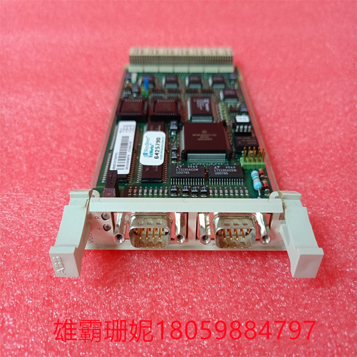
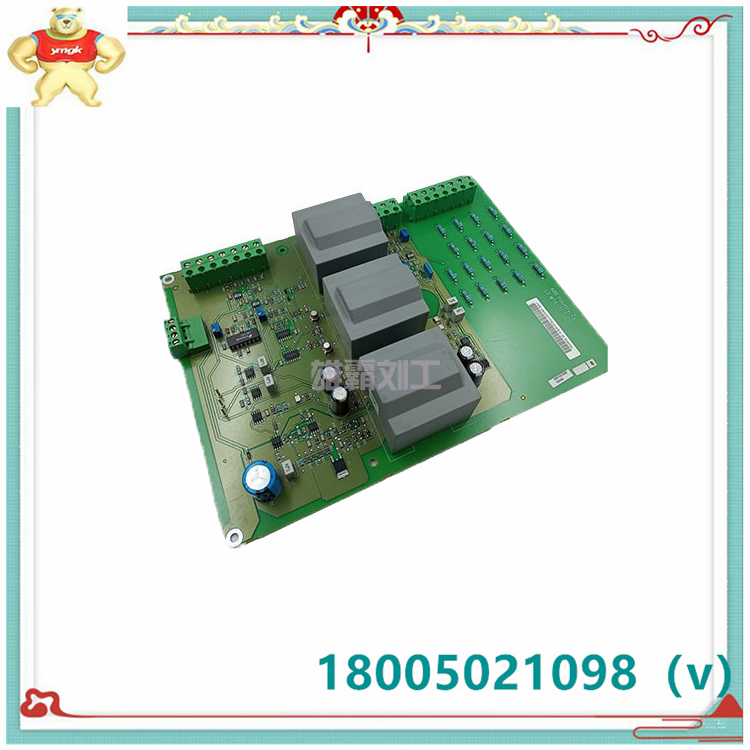
CI532V05 3BSE007297R1 ABB 模块卡件
CI532V05 3BSE007297R1 ABB 的软件设计根据硬件结构的总体划分,也可以分为两大部分来描述。整个系统的运行如图2所示,FPGA和DSP各自的程序独立运行,通过中断信号完成数据的实时交互。FPGA向DSP方向的指令是通过FPGA发送一个EDMA请求,DSP通过响应EDMA请求,建立EDMA通道,开始从FIFO中进行预处理后数据的读取,DSP向FPGA传输数据时,通过向FPGA发送一个中断信号,让其从FIFO中把压缩后的图像数据读出来。
CI532V05 3BSE007297R1 ABB 系统工作流程可以简单描述如下:系统上电后,首先DSP由flash实现自举,并运行引导程序,之后转入EDMA等待状态,FPGA初始化后等待外部图像采集命令,收到图像采集命令后开始进行图像采集,并对采集到的图像进行预处理,预处理后的图像经过FIFO缓冲,在存储一定量的数据之后,FPGA通过半满信号向DSP发送EDMA请求,等待DSP响应,DSP一旦收到来自FPGA的EDMA请求,立即建立EDMA通道,从FIFO中读取数据到L2存储器,存满一帧图像后DSP开始图像压缩,等待一幅图像压缩完成之后,DSP会向FPGA发送中断信号,FPGA在收到中断信号后开始从 FIFO中读取压缩后的图像数据。一帧数据读完后,判断编码信号是否有效,如果有效则按同样的规则对下一帧图像进行压缩,如果无效则通知DSP结束。
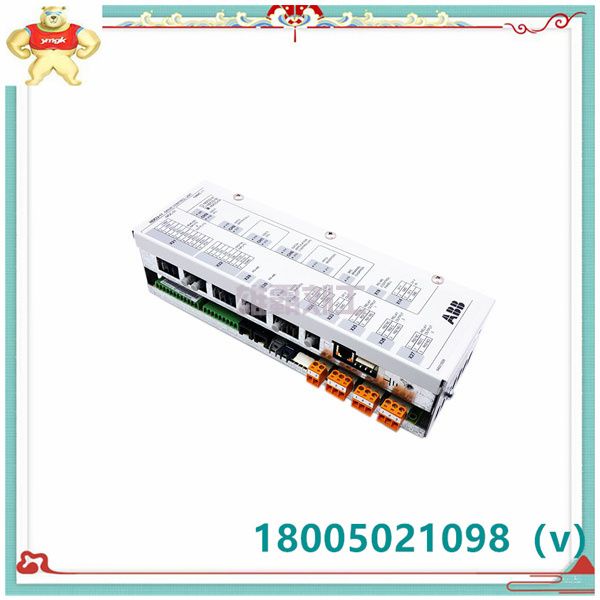
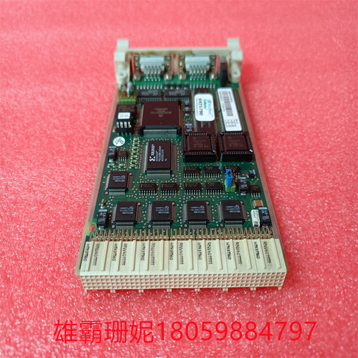
CI532V05 3BSE007297R1 ABB 模块卡件
CI532V05 3BSE007297R1 ABB's software design can also be divided into two parts to describe according to the overall division of the hardware structure. The operation of the whole system is shown in Figure 2. The programs of FPGA and DSP run independently and complete real-time data interaction through interrupt signals. The instruction from FPGA to DSP is to send an EDMA request through FPGA, and the DSP establishes an EDMA channel in response to the EDMA request and starts to read the pre-processed data from the FIFO. When the DSP transmits data to the FPGA, it sends an interrupt signal to the FPGA. Let it read the compressed image data out of the FIFO.
CI532V05 3BSE007297R1 ABB system workflow can be simply described as follows: After the system is powered on, the DSP is bootstrapped by flash first, and the boot program is run, and then it is transferred to the EDMA waiting state. After initialization, the FPGA waits for the external image acquisition command. After receiving the image acquisition command, the image acquisition begins, and the acquired image is preprocessed. After storing a certain amount of data, FPGA sends EDMA request to DSP through half-full signal, waiting for DSP response. Once DSP receives EDMA request from FPGA, it immediately establishes EDMA channel, reads data from FIFO to L2 memory, and starts image compression after storing one frame of image. After an image compression is completed, the DSP sends an interrupt signal to the FPGA, and the FPGA begins to read the compressed image data from the FIFO after receiving the interrupt signal. After reading a frame of data, the encoded signal is judged whether it is valid. If it is valid, the next frame image is compressed according to the same rules. If it is invalid, the DSP is notified to end.
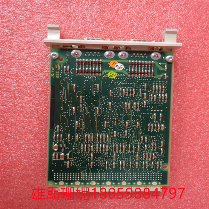
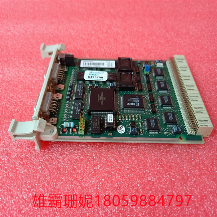
CI532V05 3BSE007297R1 ABB 模块卡件

| ABB | UFC760BE1142 |
| ABB | UFC760BE142 |
| ABB | UFC760BE42 |
| ABB | UFC760BE41 |
| ABB | KUC755AE105 3BHB005243R0105 |
| ABB | KUC755AE106 3BHB005243R0106 |
| ABB | 3BHL000986P7000 LXN1604-6 |
| ABB | 3BHE032285R0102 XVC772 A102 |
| ABB | PM861AK01 |
| ABB | 5SHX1960L0004 |
| ABB | CI854K01 3BSE025961R1 |
| ABB | TC560V2 3BSE022178R1 |
| ABB | TC625 |
| ABB | PFEA111-20 3BSE028140R0020 |
| ABB | DDC779CE102 3BHE027859R0102 |
| ABB | DDC779BE02 3BHE006805R0002 |
| ABB | UAC383AE01 |
雄霸工控

微信二维码
Copyright © 2022-2024 厦门雄霸电子商务有限公司 版权所有 备案号:闽ICP备14012685号-33