
全国咨询热线
全国咨询热线

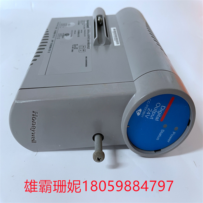


HONEYWELL CC-PDOB01 控制器备件
CC-PDOB01霍尼韦尔有许多参数,可以进行配置以满足特定的应用要求。这些参数包括:
输出类型:CC-PDOB01霍尼韦尔模块支持下沉和源输出类型。此参数可以使用模块的配置软件进行设置。输出电流:每个通道的最大输出电流可以使用模块的配置软件配置在0.5 A和2 A之间。输出延迟:可以使用模块的配置软件以毫秒为单位配置每个通道的输出延迟。该模块支持一系列输出配置,包括脉冲输出、锁存输出和故障保护输出。这些配置可以使用模块的配置软件-输出配置:进行设置。
CC-PDOB01霍尼韦尔是一款多功能、可靠的数字输出模块,适用于各种工业应用。其可配置的参数使其易于适应特定的应用要求,而其稳健的设计确保了在恶劣环境中的可靠性能
FPGA向DSP方向的指令是通过FPGA发送一个EDMA请求,DSP通过响应EDMA请求,建立EDMA通道,开始从FIFO中进行预处理后数据的读取,DSP向FPGA传输数据时,通过向FPGA发送一个中断信号,让其从FIFO中把压缩后的图像数据读出来。 整个系统工作流程可以简单描述如下:系统上电后,首先DSP由flash实现自举,并运行引导程序,之后转入EDMA等待状态,FPGA初始化后等待外部图像采集命令,收到图像采集命令后开始进行图像采集,并对采集到的图像进行预处理,预处理后的图像经过FIFO缓冲,在存储一定量的数据之后,FPGA通过半满信号向DSP发送EDMA请求,等待DSP响应,DSP一旦收到来自FPGA的EDMA请求,立即建立EDMA通道,从FIFO中读取数据到L2存储器,存满一帧图像后DSP开始图像压缩,等待一幅图像压缩完成之后,DSP会向FPGA发送中断信号,FPGA在收到中断信号后开始从 FIFO中读取压缩后的图像数据。一帧数据读完后,判断编码信号是否有效,如果有效则按同样的规则对下一帧图像进行压缩,如果无效则通知DSP结束。 3结论 本设计方案已经经过了硬件验证,达到了预定的设计要求,实现了大数据量的实时处理。 系统体积仅为70×70mm,功耗小于5W,中值滤波速率平均20F/S,JPEG压缩速率平均25F/s以上。不仅满足了视频处理系统的实时性要求,且体积小、功耗低,而且基于FPGA的可编程性,本系统具有良好的灵活性和扩展性。
HONEYWELL CC-PDOB01 控制器备件
CC-PDOB01 Honeywell has many parameters that can be configured to meet specific application requirements. These parameters include:
Output type: CC-PDOB01 Honeywell module supports sink and source output types. This parameter can be set by using the configuration software of the module. Output current: The maximum output current of each channel can be configured between 0.5 A and 2 A using the configuration software of the module. Output delay: You can use the module's configuration software to configure the output delay of each channel in milliseconds. The module supports a series of output configurations, including pulse output, latch output and fault protection output. These configurations can be set using the module's configuration software-Output Configuration:.
CC-PDOB01 Honeywell is a multifunctional and reliable digital output module, which is suitable for various industrial applications. Its configurable parameters make it easy to adapt to specific application requirements, and its robust design ensures reliable performance in harsh environments.
MB86S02 video image sensor collects video image information under the control of FPGA. After receiving the acquisition command from PC, MB86S02 starts to collect video signals. As the core control unit of the system, FPGA is not only responsible for the collection of video images, but also for the preprocessing of video image information and the data interaction among all units and modules of the system. In view of the large amount of video image data, in order to ensure the real-time requirements of the system, the system uses a large-capacity off-chip SDRAMMR to cache the collected video image information, and the SDRAM controller is realized by FPGA. After the video image information is cached by SDRAM, it must be filtered by FPGA to eliminate the noise interference in the image information. In this system, the collected video information is processed by median filtering, and the filtered data enters the DSP through the internal FIFO of FPGA for further compression. After the DSP is powered on, it first loads the boot program and waits for the FPGA to send a request. After receiving the request from the FPGA, the DSP establishes an EDMA channel to obtain video data from the FPGA, and after storing a full frame, it starts JPEG compression of the video image. After the compressed video image information is buffered by the FIFO, it is written into the data buffer area of the USB interface controller under the control of the FPGA, waiting for the reading request of the PC. The USB interface controller writes the data into port 1 of PDIUSBD12 after receiving the reading request from the PC, so that the PC can read the data next. 2 Overall design of system software According to the overall division of hardware structure, the software design of the system can also be described in two parts. The operation of the whole system is shown in Figure 2. The programs of FPGA and DSP run independently, and the real-time interaction of data is completed through interrupt signals. The instruction from FPGA to DSP is to send an EDMA request through FPGA. DSP responds to the EDMA request, establishes an EDMA channel, and starts to read the preprocessed data from FIFO. When DSP transmits data to FPGA, it sends an interrupt signal to let it read the compressed image data from FIFO. The workflow of the whole system can be simply described as follows: after the system is powered on, first, the DSP is bootstrapped by flash, and the boot program is run, and then it turns to the EDMA waiting state. After the FPGA is initialized, it waits for the external image acquisition command, and after receiving the image acquisition command, it starts to acquire the image, and preprocesses the acquired image. The preprocessed image is buffered by FIFO, and after storing a certain amount of data, The FPGA sends an EDMA request to the DSP through a half-full signal, waiting for the DSP to respond. Once the DSP receives the EDMA request from the FPGA, it immediately establishes an EDMA channel, reads data from the FIFO into the L2 memory, and starts image compression after a frame of image is filled. After an image compression is completed, the DSP sends an interrupt signal to the FPGA, and the FPGA starts reading the compressed image data from the FIFO after receiving the interrupt signal. After reading a frame of data, it is judged whether the coded signal is valid. If it is valid, the next frame of image is compressed according to the same rules. If it is invalid, it is notified to DSP to end. Conclusion This design scheme has been verified by hardware, achieved the predetermined design requirements, and realized the real-time processing of large data. The volume of the system is only 70×70mm, the power consumption is less than 5W, the average median filtering rate is 20F/S, and the average JPEG compression rate is above 25 F/s.. It not only meets the real-time requirements of video processing system, but also has small volume and low power consumption. Based on the programmability of FPGA, this system has good flexibility and expansibility.
HONEYWELL CC-PDOB01 控制器备件
HONEYWELL FC-TSDO-0824
HONEYWELL FC-PSU-240516
HONEYWELL FC-TSGAS-1624
HONEYWELL 396352-01-4
HONEYWELL 05701-A-0301
HONEYWELL HCIX15-TE-FA-NC
HONEYWELL SDOL-0424
HONEYWELL 05704-A-0146
HONEYWELL HCIX15-TE-FA-NC 保护膜 触摸板
HONEYWELL 05701-A-0302
HONEYWELL CC-TCNT01
HONEYWELL FC-SDO-0824 V1.3
HONEYWELL FC-SAI-1620M
HONEYWELL CC-PAIH02
HONEYWELL CC-PFB401
HONEYWELL CC-TDIL01
HONEYWELL TK-CCR014
HONEYWELL CC-PAIM01
HONEYWELL FBM201
HONEYWELL CC-PFB401
HONEYWELL CC-TAIX01
HONEYWELL CC-PCF901
HONEYWELL TERMINAL PLATE F860-CA
HONEYWELL CC-PCNT01
HONEYWELL CC-PAIH02
HONEYWELL FC-FANWR-24R
HONEYWELL 51199929-100
HONEYWELL 05701-A-0302
HONEYWELL CC-PCF901
HONEYWELL CC-TDIL01
HONEYWELL CC-PAOH01
HONEYWELL FC-PSU-UNI2450U V1.0
HONEYWELL 3BHB040288R0001
HONEYWELL 3BHB009183P0001
HONEYWELL 05701-A-0301
HONEYWELL FC-PSU-UNI2450U V1.0
HONEYWELL CC-PDIS01
雄霸工控

微信二维码
Copyright © 2022-2024 厦门雄霸电子商务有限公司 版权所有 备案号:闽ICP备14012685号-33

